PVD Blog

PVD Staff

Recent Posts

More than a Motto: Designing a Recipe for Deposition System Success

For decades, PVD has been the leader in designing and building custom deposition systems. Our motto is "Creativity, Collaboration, Communication." What does that mean for our customers? Below we outlined how each of these words are applied into our process daily and how it translates into customer success.
Read More

Deposition System Design: Considerations for Ion Beam Source Selection

Ion sources can be used for a variety of applications in thin film deposition and etching. For example, they can be used for substrate pre-cleaning, reactive deposition of oxide and nitrides (ion beam assisted deposition), and ion beam milling. When selecting and designing a deposition system that uses an ion source, many factors come into play. Some design features are dictated by the application, and some can be balanced against cost and performance. Below are five factors to keep in mind as you select an ion beam source.
Read More

Advancing Thin Film Deposition Methodology: Three Factors for High Throughput Deposition

Complex coating processes, such as combinatorial sputter deposition and pulsed laser deposition (PLD), require significant attention to detail, and successful results rely on quality equipment. PVD Products is continually developing innovative solutions to overcome common technical challenges that accompany newer processes for PLD and combinatorial deposition. The following improvements are three examples of these solutions:
Read More

The Material Discovery Funnel: A Six-Step Process for Advanced Material Development

The forward march of technology relies on continuous improvement of critical components such as semiconductors, batteries, fuel cells, and the like. In time, every component runs up against performance constraints established by fundamental physics and chemistry. Overcoming those restrictions requires the development of unique
Read More

Meet the Team: Larry Margagliano, Principal Engineer

Before joining the PVD Products team, Larry Margagliano developed his engineering background in various industries. Considering himself a master engineer, Margagliano has been on the management side of projects as well as implementation. He has experience setting the technical approach, doing the hands-on work, and having the final project sign-off. Below, Margagliano shares what it's like to learn a new technology and key considerations for system design.
Read More

Service After the Sale: Extending the Life and Function of Your Custom Deposition System

At PVD, installing a custom deposition system at a customer’s facility signals the beginning—rather than the end—of that customer relationship. We’ve been known to return months and even decades later to upgrade or service a tool, expanding the utility of our thin film deposition systems.
Read More

System Control Software: Developing Your Custom Deposition Program

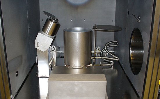
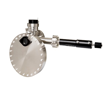
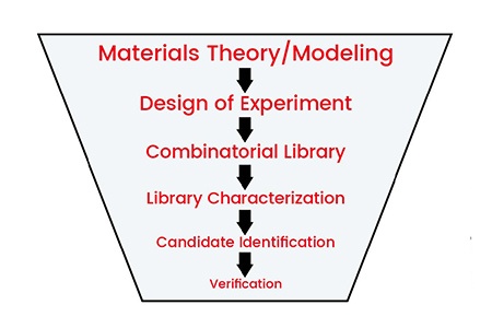
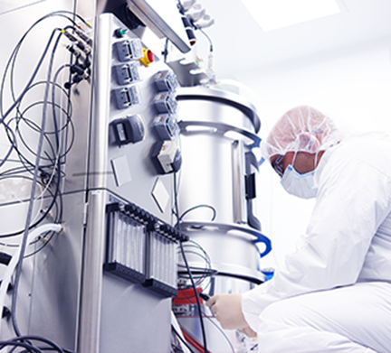
A customized deposition system can help you achieve the best results with maximum efficiency. For example, a well-designed combinatorial deposition system can execute a program to produce a wide range of slightly different film compositions, each deposited within discrete test pads on a single substrate. This makes it possible to explore an enormous range of material combinations and structures within a single wafer run. Effective combinatorial deposition experiments require precise control over several deposition parameters, such as selection from multiple magnetrons and types of power supplies, target-to-substrate distance, mass flows from multiple MFCs, pressure, test pad exposure time, and exact substrate position. With full control of all parameters, practically any desired recipe can be executed within each test pad.
Read More

Valentine’s Day: What Does It Have To Do with Sputtered Thin Films

PVD Products teamed up with Tin Model, LLC to explain the connection between magnetron sputtering processes and Valentine's Day. Thin-film materials deposited via sputtering processes can vary widely both in properties and in thickness distribution. This is partially because vapor plumes emanated from magnetron sputtering sources can take various shapes, depending on the design of the magnetron, the material, the state of erosion and other influencers.
Read More

Case Study: Increasing Vacuum Coating Capacity for a Leading Optical Component Manufacturer

In Spring 2015, PVD started working with a customer who specialized in providing and manufacturing subsystems, process controls, and instruments for markets using thin film technology. In their search for a new vendor who could build a vacuum coater to their detailed specifications, the customer solicited ten companies. Out of those ten companies, PVD was selected for the project. Recently, we spoke with the customer about the process of working with PVD. They told us:
Read More

Meet the Team: Larry Scipioni, Chief Technology Officer

Before joining the team at PVD Products, Larry Scipioni got to know the company as a customer. During that time, he took an interest in PVD’s large-scale, high-complexity work, which aligned with his graduate work in thin film deposition. "I'd love to work there," he thought.
Read More
 
Site Meter