PVD Products designs and manufactures high-performance Pulsed Laser Deposition (PLD) Systems for researchers and engineers developing next-generation materials, thin films, and functional coatings. Our PLD platforms are trusted by leading universities, national labs, and advanced manufacturing teams worldwide for applications requiring exceptional film purity, stoichiometric transfer, and atomic-level control.
Whether you are depositing complex oxides, nitrides, superconductors, ferroelectrics, or novel semiconductor materials, PVD Products delivers precision-engineered PLD systems that scale from fundamental research to pilot production.


No two research programs are the same. That is why PVD Products offers fully customized PLD systems, including:
Load-lock and cluster tool configurations
Multiple laser ports and beam delivery options
Multi-chamber deposition and analysis systems
Hybrid PLD + sputtering + evaporation platforms
Glovebox-integrated and inert-atmosphere systems
Each system is designed in close collaboration with your team to ensure perfect alignment with your materials, processes, and long-term roadmap.

Our very popular low-cost Nano PLD system is designed for researchers interested in small-scale thin film materials development and is high pressure RHEED compatible. This system can handle wafers up to 2 inches (50.4 mm) in diameter as well as smaller samples. Though this is our most basic system, the Nano PLD doesn’t compromise onmany of the key features of our larger area and more sophisticated PLD systems.

Polymer deposition from a vapor phase produced by laser ablation requires the use of low energy photons in the Visible to Near Infrared (VIS/NIR) range of wavelengths. PVD Products offers two approaches to PLD polymer films, Matrix Assisted Pulsed Laser Evaporation (MAPLE) and VIS/NIR Resonant Infrared Absorption. Both systems are based on our Nano PLD chamber design.

PLD/MBE 2100, 2300, and 2500 systemsoffer the user a wide choice of features that cannot be matched by any other PLD systems on the market today. These systems are designed specifically to grow epitaxial films, mono-layer by mono-layer film structures, and/or combinatorial thin films and can easily be integrated with a wide variety of other deposition techniques and sources.

Femto and pico second PLD systems provide efficient coupling to target materials, resulting in very high deposition rates. In addition, femto and pico second PLD systems may significantly reduce particulate sizes under the proper conditions. PVD Products can provide complete PLD systems based on our standard designs including Nano PLD, the PLD/MBE series, and large area PLD systems. These systems are available including a variety of lasers with a wide range of power levels to meet your specific needs.

Our Nano PLD, PLD/MBE series, or larger PLD deposition systems provide a complete PLD combinatorial thin films PLD solution. Custom systems can be provided as well.

PVD Products can help with the design and science behind your production coating process, right from the start. Our PLD Production Systems are capable of depositing high quality uniform films on substrates up to 12 inches in diameter.
PLD ComponentsPVD Products provides a full array of PLD components for your custom PLD tool. Our PLD components will be specifically designed for your custom or OEM PLD system, and 3-D solid models will be provided for approval before the manufacture of the customized parts. In most cases, we can retrofit our components to most custom or other OEM systems.
We provide a full range of PLD coating systems designed to deliver precise, high-quality thin-film deposition for research, pilot, and production applications. Our systems handle substrates from small research wafers up to large 8–12 inch production pieces and include advanced options such as hybrid PLD/MBE configurations, femtosecond and picosecond laser setups, and MAPLE (Matrix Assisted Pulsed Laser Evaporation) for delicate or polymer materials. In addition to the coating systems themselves, we supply sources and customizable components, and we often integrate PLD with complementary technologies like magnetron sputtering, thermal and e-beam evaporation, and ion sources, enabling tailored, application-specific thin-film solutions from the lab to full-scale production.
Our PLD services support every stage of thin-film development, from research and prototyping to pilot and full-scale production. Our services include custom thin-film deposition using Pulsed Laser Deposition on a wide range of substrates, process optimization to achieve precise film thickness and uniformity, and material-specific solutions such as oxide, metallic, or polymer coatings. In addition, we provide thin-film characterization and post-deposition treatments to ensure films meet exact performance specifications. By combining our PLD expertise with complementary technologies like sputtering, evaporation, and ion beam deposition, we deliver end-to-end solutions that help our customers accelerate development and achieve high-quality, reproducible thin films for their applications.
Our PLD + Sputtering deposition capabilities combine the precision of Pulsed Laser Deposition with the versatility of magnetron sputtering to create high-quality thin films. This approach allows us to deposit metals, oxides, and complex materials with excellent uniformity, adhesion, and controllable thickness across a wide range of substrates. Our systems can be configured for research, pilot, or production-scale applications, and we offer process optimization and post-deposition treatments to meet specific material and performance requirements. By integrating PLD with sputtering and complementary deposition techniques, we deliver flexible, application-specific solutions that ensure reproducible, high-performance thin films for advanced research and industrial applications.
Our PLD platforms are used by leading universities, national laboratories, and industrial R&D teams worldwide to deposit high-performance, complex, and functional materials with unmatched compositional fidelity. Unlike off-the-shelf tools, PVD Products' PLD equipment is built around modular, configurable architectures that can be precisely matched to your materials, substrates, and long-term roadmap.
PLD is particularly well-suited for depositing:
Complex oxides
Nitrides
Superconductors
Ferroelectric and piezoelectric materials
Magnetic and spintronic materials
Wide bandgap semiconductors
Quantum and correlated electron materials
Because PLD preserves target stoichiometry, it is often the preferred method for materials that are difficult to deposit using sputtering or evaporation.
Yes. PVD Products specializes in multi-process and hybrid deposition platforms, including:
PLD + sputtering
PLD + evaporation
PLD + RHEED and in-situ diagnostics
Cluster tools with multiple chambers
These systems are ideal for complex device stacks and advanced materials research.
Contact us for a fully customized PLD system.
Pulsed Laser Deposition (PLD) is a physical vapor deposition (PVD) technique in which a high-energy pulsed laser ablates material from a solid target, forming a plasma plume that deposits onto a substrate. PLD is widely used for depositing complex, multi-element, and high-performance thin films with excellent stoichiometric transfer and crystalline quality.
Check out our PLD Systems Overview for more information.
PVD Products offers a complete portfolio of Pulsed Laser Deposition (PLD) equipment covering everything from compact research systems to pilot and full production platforms, as well as hybrid and fully custom deposition systems. Their PLD equipment is used by universities, national laboratories, and advanced industrial R&D teams worldwide.
The PLD equipment portfolio includes:
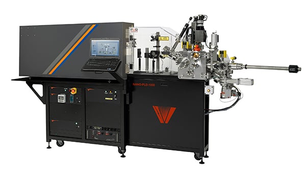
Nano PLD systems are designed for early-stage research, materials discovery, and small substrate deposition. These systems provide full PLD capability in a compact, cost-effective platform and are ideal for:
University research labs
Exploratory materials research
Small substrate and proof-of-concept thin films
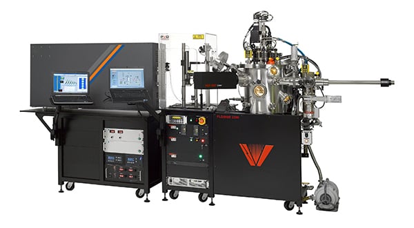
These are the most widely used PLD platforms for advanced materials development and process scale-up. They support:
High-quality uniform thin films
Multi-target deposition
Combinatorial and multilayer structures
Substrates from small samples up to medium wafer sizes
These systems are commonly used for complex oxides, superconductors, functional ceramics, and semiconductor materials research.
Production PLD systems are designed for larger substrates, higher throughput, and repeatable manufacturing processes. They offer:
Large-area deposition capability
Advanced thermal management
High uniformity across large substrates
Support for multi-wafer or large-format substrates
These systems are used for pilot production, device fabrication, and specialized manufacturing applications.
PVD Products offers hybrid PLD and Molecular Beam Epitaxy (MBE) systems for applications that require:
Ultra-high vacuum environments
Monolayer-level growth control
Advanced epitaxial film growth
In-situ diagnostics such as RHEED
These platforms are widely used in quantum materials, oxide electronics, and advanced heterostructure research.
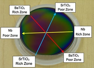
These PLD systems are optimized for:
High-throughput materials discovery
Composition-spread libraries
AI-driven and data-driven materials research
Rapid screening of new material systems
They enable researchers to explore entire material families on a single substrate.
PVD Products also offers specialized PLD variants, including:
MAPLE (Matrix-Assisted Pulsed Laser Evaporation) systems for polymers and soft materials
Systems optimized for VIS/NIR laser sources
Systems designed for non-traditional or sensitive materials
In addition to standard platforms, PVD Products designs and builds fully custom PLD systems, including:
Multi-chamber cluster tools
Glovebox-integrated systems
Hybrid PLD + sputtering + evaporation platforms
Application-specific chambers, substrates, and environments
"PVD doesn’t work in a transactional sense; they give and provide information when we need it."