Quickly optimize film composition. Our Nano PLD, PLD/MBE series, or larger PLD deposition systems provide a complete PLD combinatorial thin films PLD solution.
Compositional gradients can be created via software routines and/or using programmable masks. Binary, tertiary, quaternary, etc. combinatorial films can be easily grown.
Custom systems can be provided as well. Check out our sputtering combinatorial deposition tools.
As an example of a combinatorial thin film, below is a photograph of a 2-inch silicon wafer with a combinatorial film grown using BaTiO3, SrTiO3 and Nb targets. This film is nominally 200 nm thick, and the chemical composition varies considerably from an elemental "rich" zone to a "poor" zone directly across the wafer.

2-inch diameter Si wafer with a 250-nm thick tertiary combinatorial film
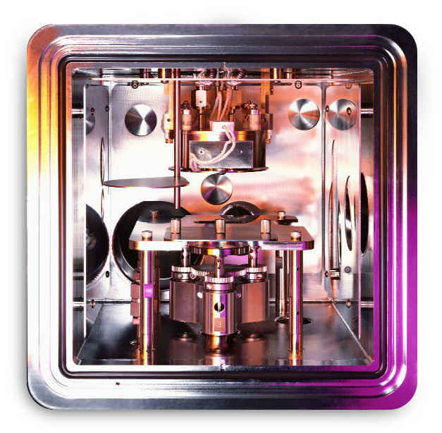
Below is a "wafer’s eye view" of a combinatorial thin film system using masks mounted on programmable actuators. The mask holders are designed to hold metal masks with various cutouts to produce a thickness gradient of a given material in the deposited thin film.
Utilizing multiple targets and masks, one can produce a variety of compositional gradients on a wafer surface in a short amount of time. Also shown is the location of the "active" 1-inch diameter ablation target pedestal in this six-target Nano PLD system. The pedestal is sitting below the water-cooled plate.

Combinatorial thin film system from the wafer’s point of view
Download our free eBook for an overview of current combinatorial deposition methods and introduction of five developments our team has made to improve these methods.