33.jpg

Solution-Deposition Planarization (SDP)

Solution-Deposition Planarization (SDP) is a relatively new method of producing a smooth surface (< 2 nm), which has several advantages over traditional techniques such as  electropolishing (EP) or mechanical polishing. PVD Products and Dr. Vlad Matias of iBeamMaterials, Inc. have jointly developed a solution-deposition planarization process and manufacturing tool for production of 100-200 meter long tapes and up to 10 cm wide rolls.

AFM scan of yttria coated Hastelloy tape with less than 1 nm surface roughness >

Key components of the SDP tool

High temperature superconducting wires are made from a coated conductor wound around a cooled core material. The coated conductor typically starts with a 10-100 mm wide Hastelloy tape, followed by a yttria barrier layer, an oriented MgO nucleation layer, a YBCO high Tc film, and a thick overcoat of silver. The quality of the film stack is highly dependent on an exceptionally smooth surface beneath the MgO.

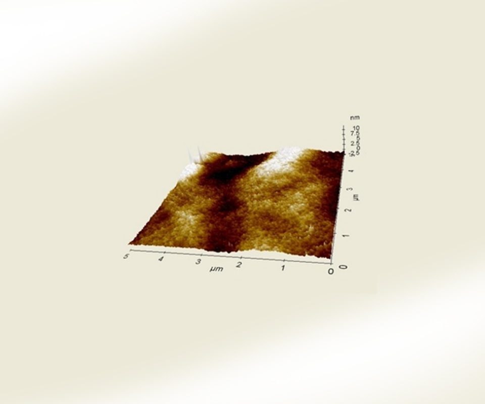
The tape makes multiple passes through a series of proprietary coating baths and high temperature furnaces to produce an extremely smooth yttria surface suitable for deposition of an oriented MgO nucleation layer.

Model of the solution-deposition planarization reel-to-reel system

This prototype system allows for coating of tapes up to 11 cm wide and up to 200 meters in length.

Solution-deposition planarization reel-to-reel system

IBAD-MgO studies were performed on two series of samples. Overall results show good quality texture as expected in smooth coatings. The RHEED image shown here is indicative of the quality of the homoepitaxial growth that can be obtained with SDP tapes.

PVD Products can provide you with a solution deposition planarization system to meet your specific requirements.

RHEED image of a good quality thin MgO homoepitaxial layer

Customize A System

Do you know the specifications you need to reach?
Contact us to discuss a custom system.

Site Meter