
In Part 1 of our deposition rate and uniformity series, we discussed the key considerations for deposition tool performance. The second part of our series takes a look at the steps for deposition system design based on rate and uniformity.
 A common sputter deposition design challenge is seen in the simple deposition of metallic thin films. Two metals that commonly are utilized in the same system are gold (Au) and titanium (Ti), the latter serving as an adhesion layer for the former. These two materials differ greatly, however, in their behavior as sputter targets. Au has a sputter yield which is 3.5 times that of Ti – that is, the number of atoms ejected for every ion of process gas that strikes the target – and can handle twice the operating power of Ti due to its higher thermal conductivity. A Ti target will overheat more quickly before the expended power can be drawn away by the unit’s cooling water.
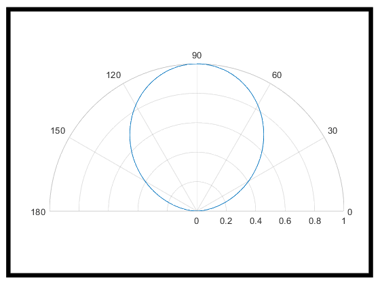
This has two consequences. First, even with the same magnetron, power source and geometry, one cannot achieve the same deposition rate with Ti as with Au. In fact, the magnetron could be seriously damaged if an attempt were made to run Ti at the same conditions as Au. Second, each target material has its own emission pattern, which is the amount of flux coming out of the source as a function of angle. This will impact the uniformity of the deposition across a given substrate area. Figure 1 shows the differing angular emission patterns of Ti and Au, based upon literature[1] values. Note that materials with higher sputter yield tend to have narrower angular distributions.
![]()
![]()
![]()
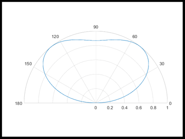
Figure 1. Sputter target emission flux vs. angle for Au (left) and Ti (right). 90° mark is perpendicular to target surface
Arriving at the Best System Design
In light of these complexities, modeling is a critical tool to guide design choices and meet tool specifications. In an existing instrument, models can help predict the outcome of a coating run, reducing the number of trial-and-error measurement cycles. Even a simple example can highlight the insights gained.
Figure 2 shows a typical confocal sputtering geometry using a 2” diameter magnetron with a 100-mm diameter wafer, as represented in modeling software. In this sputter-up configuration, the front face of the target is seen pointing up, centered on a radial point halfway from center to edge of the substrate. The geometry of the system and the emission characteristics of the target are set as parameters. The blue dots on the substrate circle are selected analysis points. In order to model deposition rate and uniformity, the flux received at each point is found by numerical integration over the target surface and over a 360° range of substrate rotation angle.
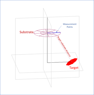 Figure 2. 3D sketch of sputter coating geometry for a 2” magnetron and 100-mm diameter wafer, generated within the V-Grade 5S software. [2]
Results
Results of the modeling are shown in Figure 3 and in Table 1. While the deposition rate for Ti is 8x lower, the uniformity is much better. The broad emission profile gives a wider central spot to the deposition pattern. While the uniformity can certainly be improved by increasing the Au target-substrate distance, as is done in evaporation, more precious metal is then wasted to the shields. It would be more beneficial to change the angle of the magnetron in addition to the distance. Alternatively, the requirements may drive the design to incorporate a larger magnetron or shadow masks to address this problem.
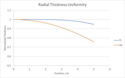
Figure 3. Deposition uniformity modeling predictions for a 100-mm target-substrate distance, with a 2” diameter magnetron.
Table 1. Deposition rates for the confocal sputtering system from a 2” diameter target.
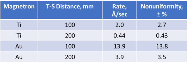
Table 1. Deposition rates for the confocal sputtering system from a 2” diameter target.
From the results, we see that no one configuration is suitable for all deposition tasks. It is generally not possible to create a system that meets one given rate and uniformity specification for any material at all possible target-substrate distances that the machine is physically capable of reaching. However, smart design choices and predictive modeling help to optimize the conditions per application. In Part 3 of our series, we will give an example of deposition design with linear substrate motion for a tape-coating application.
At PVD Products, we design custom-made thin film deposition systems to meet your specific requirements based on desired material properties and process complexity, range of substrate size, manufacturing tolerances and throughput requirements. Contact us for planning and design guidance:

[1] Martynenko et al., Technical Physics, 2012, Vol. 57, No. 4, pp. 439–444.
[2] From Tin Model, LLC. Cambridge, MA, USA
Leave a Comment