PVD Products' combinatorial sputtering systems are used for growing multiple individual thin film test pads, each with a unique composition, in a rectangular array onto substrates up to 300 mm in diameter. Each individual test pad has a uniform composition over the test pad area, as opposed to combinatorial systems with films grown using continuous compositional gradients. This approach provides for much easier electrical testing, chemical analysis, and evaluation of other film properties.

A 100 mm diameter Si wafer with an array of 64 different test pads produced by combinatorial sputtering, 4 mm square each with a different film composition. Compositions can be binary, ternary, or quaternary depending on your need and system design. Concentrations of elements can vary from less than 1 to over 99% depending on deposition conditions. Here, the materials used were Cu, Ti, V, and Al. Oxides, carbides, etc. can also be fabricated as required.

The Combo-4000 system shown includes four magnetrons with four DC power supplies, two RF power supplies, and two RF/DC switches, along with a programmable X-Y Stage and mask assembly. The system is an ideal way to create combinatorial libraries of new material compositions in a quick, programmable, and reproducible fashion. PVD can provide combinatorial deposition systems with up to six magnetrons and wafers 300 mm in diameter or larger. Systems can include single-wafer or multi-wafer load locks, localized test pad heating, and many other features.

PVD Products provides unique combinatorial sputter deposition systems to meet the customer’s thin film requirements for the creation of new material compositions. We have systems capable of providing compositional film libraries on wafers from 50 mm up to 300 mm in diameter as required. Square substrates can also easily be handled.
Our systems incorporate PVD Products' Titan Magnetrons for ease of use.

A 300 mm diameter wafer with forty-eight 25 mm square test pads, each deposited with predefined unique compositions using combinatorial sputtering.
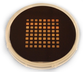
A 300 mm diameter wafer with 68 test pads deposited by combinatorial sputtering, each with a different composition, deposited over pre-patterned underlying circuitry for quick evaluation of each test pad's electrical properties. After deposition of each test pad, the wafer was then capped with a metallic layer to form the final device for electrical testing purposes.
Systems can include magnetron sputter sources with either 1.5-inch or 2-inch diameter targets, and up to four sources per system, with RF and DC capability. A wide variety of options such as MFCs for different gasses, power supply packages, single or multi-wafer load locks, etc. can be provided. Magnetrons can be mounted on Z-stages to provide a wide range and resolution of deposition rates.
Test pad sizes can range from about 4 mm square to over 25 mm square, tailored to user requirements. It is very easy to change test pad size and step-and-repeat distances in the field with our easy-to-use software.

The inside of a 300 mm diameter combinatorial sputter system, showing four magnetrons and a metal mask on a programmable vacuum-compatible stage. The mask is dropped down to within 200 microns of the wafer surface after wafer exchange. Each magnetron is also mounted on a computer-controlled Z-stage to adjust target-to-substrate distance for very fine adjustment of deposition rates.
PVD Products also makes Pulsed Laser Deposition systems, which provide wafers with continual spreads in composition as shown here in the photo of a 50 mm diameter wafer. Please see our PLD web page to learn more about these systems.

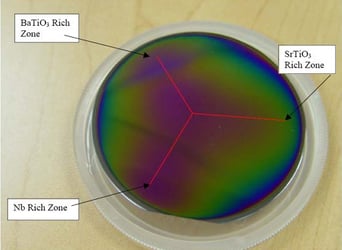
Photograph of a 50 mm diameter wafer with three materials deposited via PLD. PLD provides a continual compositional spread across the wafer surface. This is another approach to combinatorial deposition and can be conducted in all of our PLD tools.
Download our free eBook for an overview of current combinatorial deposition methods and introduction of five developments our team has made to improve these methods.