
In Part 3 of this blog series, we discussed designing deposition systems with linear substrate motion or continuous web coating. As promised, this blog will show the results of modeling of the plate coating example we defined previously.
When embarking on modeling, it is good to remember a favorite quote of ours from the computer scientist Richard Hamming: “The purpose of computing is insight, not numbers.” The ability to do a large number of experiments “in silico” helps immensely in shepherding a configuration towards an optimum and in understanding what factors are important. However, there are some caveats to be aware of in modeling performance as well. Assumptions can be performance killers if the results aren’t tied to physical reality. In our current example, the sputtering rate and the exact shape of the erosion and emission patterns for the magnetron will impact the result, so the model must be supplemented and refined by physical measurements.
Let’s briefly walk through the modeling process for our example.
1. Deposition Geometry
Figure 1 shows the geometry of the deposition, with the plate (blue) at start position over the linear magnetron (yellow). Numerical integration determines the deposition contribution at each point of the substrate, from each point on the sputter target, and for each position along the motion path. With this model, the impact of design choices on the film thickness and uniformity can be directly followed.
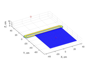
Figure 1. Deposition geometry. The deposition rate is calculated at the points in blue (substrate), arising from the modeled emission from the target (yellow). The substrate motion is going from the first red dot to the second red dot.
2. Deposition Rate
Figure 2 shows a “heat map” of the deposition rate versus position along a 15” (~40 cm) long deposition zone for two different configurations. The left panel shows that, with a 30” magnetron, the deposition tails off at the edges of the zone. This fall-off will lead to unacceptably large thickness non-uniformity. The width of the magnetron and the target-substrate (T-S) distance should be chosen to achieve the desired non-uniformity. The geometry in the right panel provides a more uniform film, which we will see next.
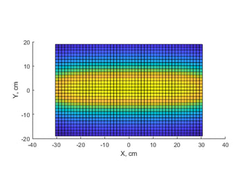
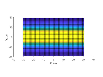
Figure 2. Heat maps of deposition rate. Left: 5” x 30” magnetron at a 4” target-substrate (T-S) distance. Right: 5” x 35” magnetron at 2” T-S.
3. Thickness vs. Position
Figure 3 shows the calculated thickness versus position, perpendicular to the substrate motion direction, for a single pass at two different T-S distances: 4” and 2”. The smaller T-S distance provides ±1.5% non-uniformity, as well as a higher axial deposition rate of 0.4nm/sec. At 2” T-S distance, the film could achieve the desired thickness in two passes, requiring just less than 5 minutes. Because the film is quite thin, better process control could be attained by increasing the substrate speed and taking more passes.
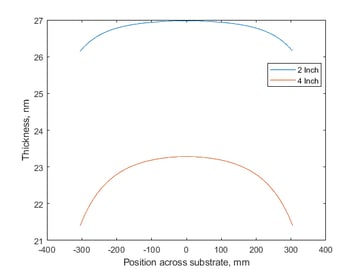
Figure 3. Thickness vs. lateral position after one pass, utilizing a 5” x 35” magnetron, for both 2” and 4” T-S distance.
4. Design Choices
Design models reveal further information. For example, the Al2O3 RF deposition rate is limited by low sputter yield and RF power that can be applied to a non-conducting target. If a thicker film is desired, throughput might be insufficient. Modeling can indicate whether it would be more economically efficient to add a second magnetron or switch to reactive deposition, which is a cheaper alternative.
5. Process Control
Performance can drift over time. The angular emission pattern usually becomes more forward-pointing as the sputtering target erodes, affecting both rate and non-uniformity. In our example, the calculated thin film deposition rate increases and non-uniformity decreases as the target erodes. The process engineer should monitor this behavior.
It is possible to extend these models to investigate curved substrates, such as drum coating or the stoichiometric uniformity in co-sputtering. For practically any geometry and process, numerical optimization can serve as a tool in the toolbox that guides instrument design to a solution that meets the application need.
Want a comprehensive look at deposition rate and uniformity? Download our eBook for the complete series.

At PVD Products we work in partnership with our customers to understand what makes for success in their research or production efforts, and we advise on the best solutions to reach their goals. Send us your specs and our engineering team will work with you to ensure you achieve optimal system design.

Leave a Comment